We know the M3 Apple Silicon chips will use the 3nm (nanometre) design process, but I wondered what happens next when they hit the nanometre limit?
AFAIUI, M3 series and maybe M4 & M5 series will use this process over the next 3years, then another 3years on 2nm (M6/7/8’s), then 3years of 1nm (M9/10/11) – but what happens after that?
That gives Apple maybe another 9-10 years of M-series Macs covered, but then where do they go for improvements? Additionally, there was some question years ago I remember reading, as to whether 2nm and or 1nm were even possible, as circuits would like bridge on the chips, as they would be so tiny as to make this occur.
I’m sure someone on here is likely much more knowledgable about the whole chip design and fabrication subject than I am, who might have more insight on this discussion point…?
Don’t be fooled by marketing BS. A “3-nm chip” has gate sizes an order of magnitude larger.
The term “3 nanometer” has no relation to any actual physical feature (such as gate length, metal pitch or gate pitch) of the transistors. According to the projections contained in the 2021 update of the International Roadmap for Devices and Systemspublished by IEEE Standards Association Industry Connection, a 3 nm node is expected to have a contacted gate pitch of 48 nanometers and a tightest metal pitch of 24 nanometers.[14] However, in real world commercial practice, “3 nm” is used primarily as a marketing term by individual microchip manufacturers to refer to a new, improved generation of silicon semiconductor chips in terms of increased transistor density (i.e. a higher degree of miniaturization), increased speed and reduced power consumption.[15][16] Moreover, there is no industry-wide agreement among different manufacturers about what numbers would define a 3 nm node. Typically the chip manufacturer refers to its own previous process node (in this case the 5 nm process node) for comparison. For example, TSMC has stated that its 3 nm FinFET chips will reduce power consumption by 25-30% at the same speed, increase speed by 10-15% at the same amount of power and increase transistor density by about 33% compared to its previous 5 nm FinFET chips.[17][18] On the other hand, Samsung has stated that its 3 nm process will reduce power consumption by 45%, improve performance by 23%, and decrease surface area by 16% compared to its previous 5 nm process.[19]
EUV faces new challenges at 3 nm which lead to the required use of multipatterning.
Siri needs to find a better reference book. Atomic radii are measured in picometers, which are 1/1000 nanometer. E.g. hydrogen is about 32 pm, gold is about 144 pm (actual radius can depend on chemical environment). Angstroms are still common for atomic measurements in chemistry, though. 1 angstrom = 100 picometers.
Yes, I know the speak of nanometre size is arbitrary marketing per company, rather than set in stone.
But OK, maybe this is somewhat mixed-up in my head somewhere(?), as I was sure I read something about running out of ‘nanometres’ to shrink to –so to speak– in the coming 5-10 years.
144 pm radii, is 288 pm diameter, or 0.244 nm, or 1 nm wire on chip would be about 4 atoms wide. I said 2 - 10 atoms wide. I stand my ground, thanks for supporting me with more data.
I think you need to apologize to Siri. You hurt her feelings.
BS Engineering Physics, MS Chemical Engineering, PhD Optical Sciences
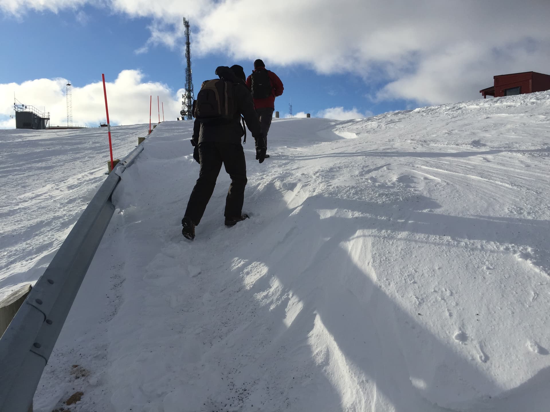
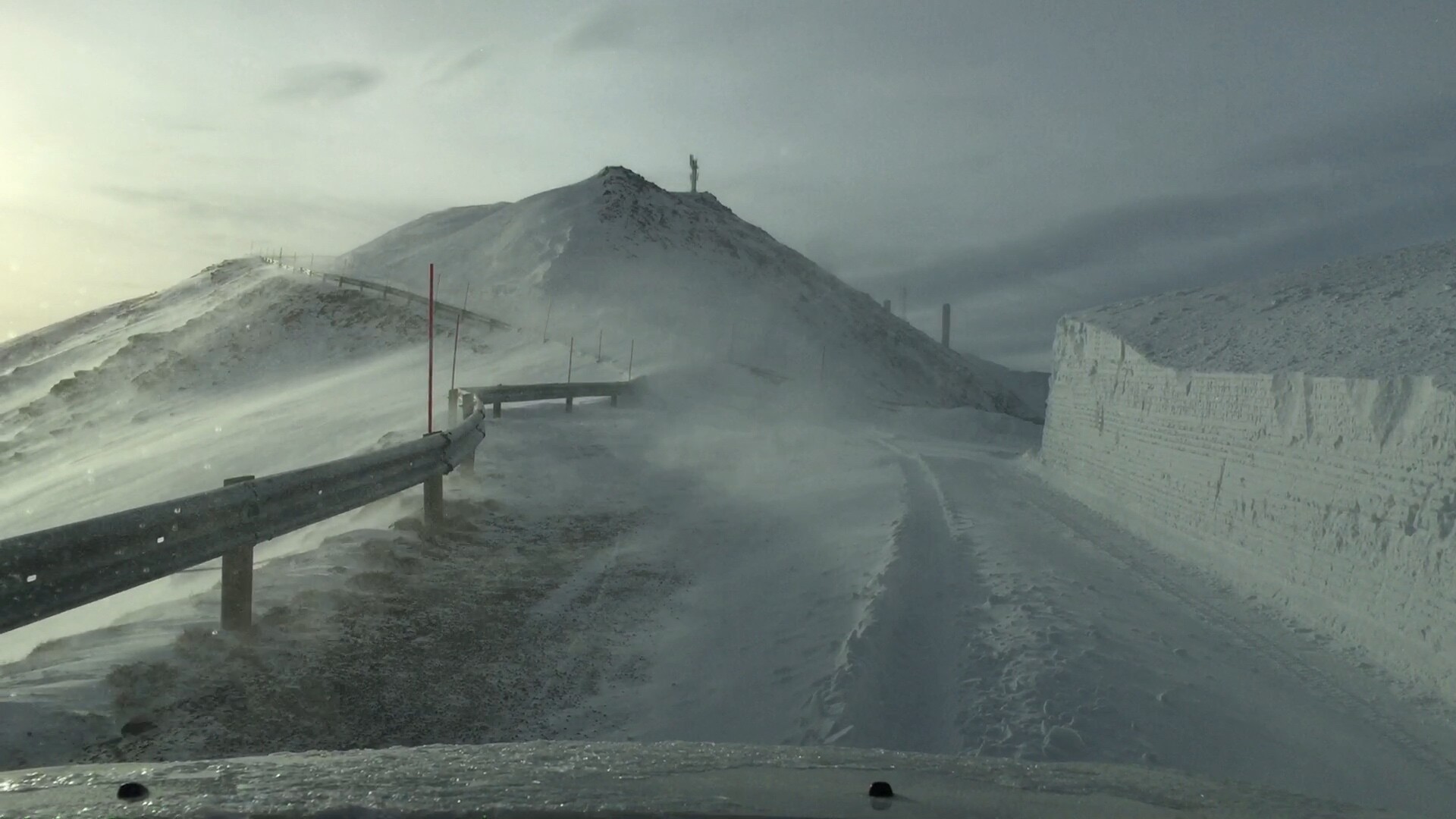
Internationally recognized Engineer for developing a coherent light source (this was a FASOR, not a laser, see Wikipedia, where wavelength had to be measured and controlled at the 7th decimal place, we did 8th) to excite atomic Sodium at 90 km altitude for Adaptive Optics (for >8 meter diameter telescopes) and first to demonstrate remote (from ground) Magnetic Field measurements at 90 km altitude, and used to measure magnetic field fluctuations during the northern lights (aurora) at Alomar Observatory, Andøya Space Center, island of Andøya, Norway, winters of 2018 - 2020, which often required crawling* 1/2 mile, uphill, in 3 - 4 feet of fresh dry powder to get to work. My grandkids have nothing to complain about! *walking and you’d just sink in to your waist, crawling and you stayed on the surface. Second photo is of road when the snow plow was working, about 2 hours after being plowed.
Seems to me that my grandparents would say something similar about complaints about the “difficulties” of getting to work/school, only they embellished it to say “uphill, both ways”.